


How Does VLSI Deisgn Shape Electronics Porduct and Its Future?
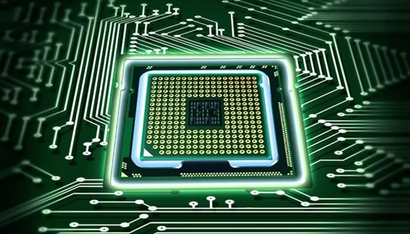
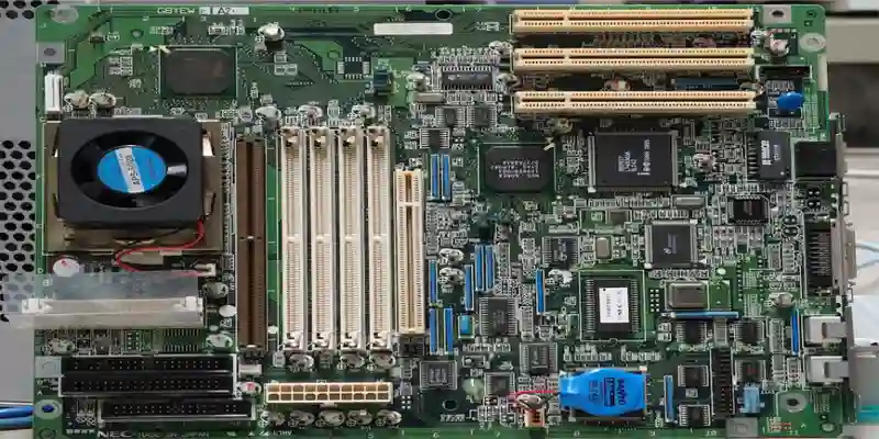
Very-Large-Scale Integration (VLSI) design is the process of creating integrated circuits by combining thousands of transistors into a single chip. These integrated circuits, also known as microchips, are present in almost all electronic devices that we use in our daily lives. From smartphones to laptops, washing machines to cars – microchips enable the functioning of modern electronics. VLSI design plays a pivotal role in advancing technology and shaping the future of electronics products. In this article, we will understand how vlsi circuit design impacts product development, enhances functionality, and drives innovation in the electronics industry.
-
Miniaturization of circuits
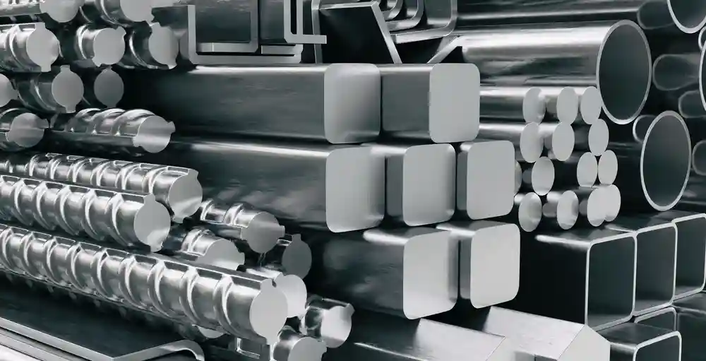
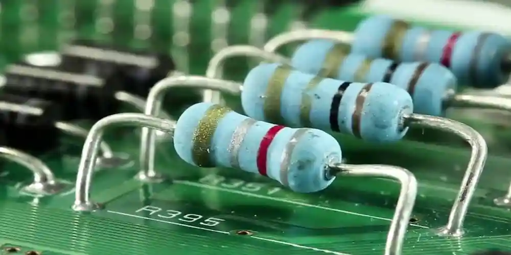
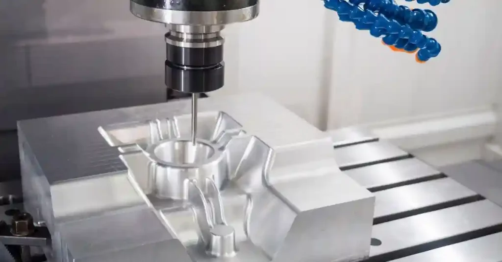
Miniaturization of circuits has been one of the most significant impacts of VLSI design. By allowing thousands of components to be integrated onto a single silicon chip, it has enabled a massive reduction in the size of electronics over the past few decades. Earlier discrete components like resistors, capacitors and transistors had to be manually wired together on large circuit boards. This resulted in electronic devices that were bulky and occupied large floor areas or entire rooms. Even simple calculators required separate boards for logic, memory and display functions.
VLSI integration changed this by packing the required components into an area smaller than a fingernail. The first microchips contained only dozens of transistors. But the density has grown exponentially according to Moore’s Law, with modern chips housing billions of transistors in the same space. This has allowed miniaturizing electronics into much smaller form factors that can be easily portable. While the first general purpose computers filled entire rooms, today a smartphone in our pocket is millions of times more powerful.
Other electronic products have seen comparable reductions in size. Miniaturization has enabled new use cases for electronics that were not possible earlier due to constraints of size and portability. Smartphones, tablets, wearables and other mobile devices have become ubiquitous consumer products. Miniaturized medical devices have improved healthcare. Advanced miniaturized sensors have enabled IoT and smart home applications.
-
Increased functionality
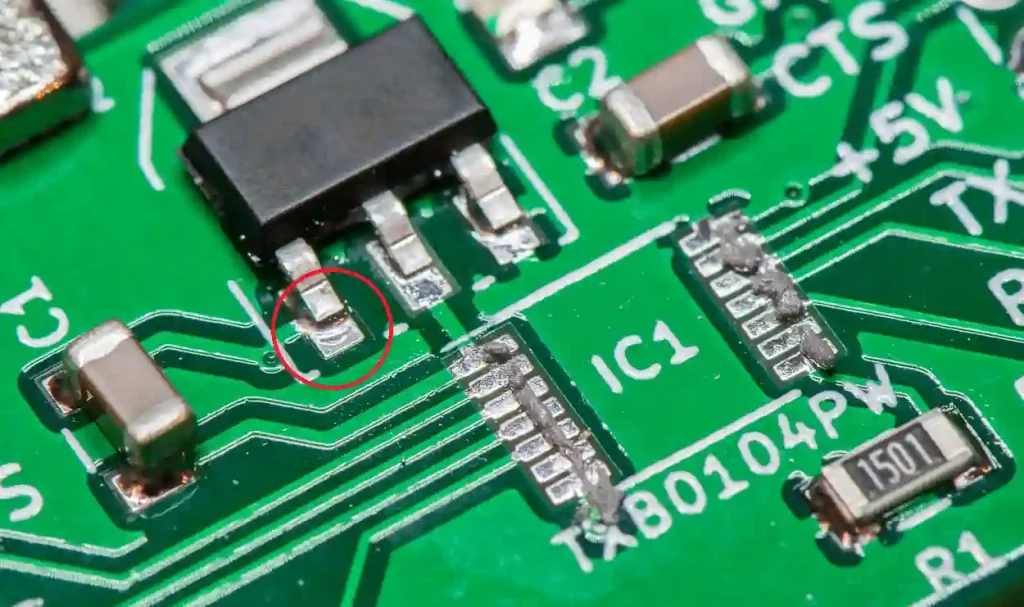
VLSI design has allowed electronics to take a giant leap in functionality by packing thousands of components into tiny silicon chips. Earlier electronic devices were limited by the number of discrete components that could be accommodated on circuit boards. This restricted the capabilities that could be delivered. However, VLSI overturned this limitation by enabling integration of entire systems on a single chip.
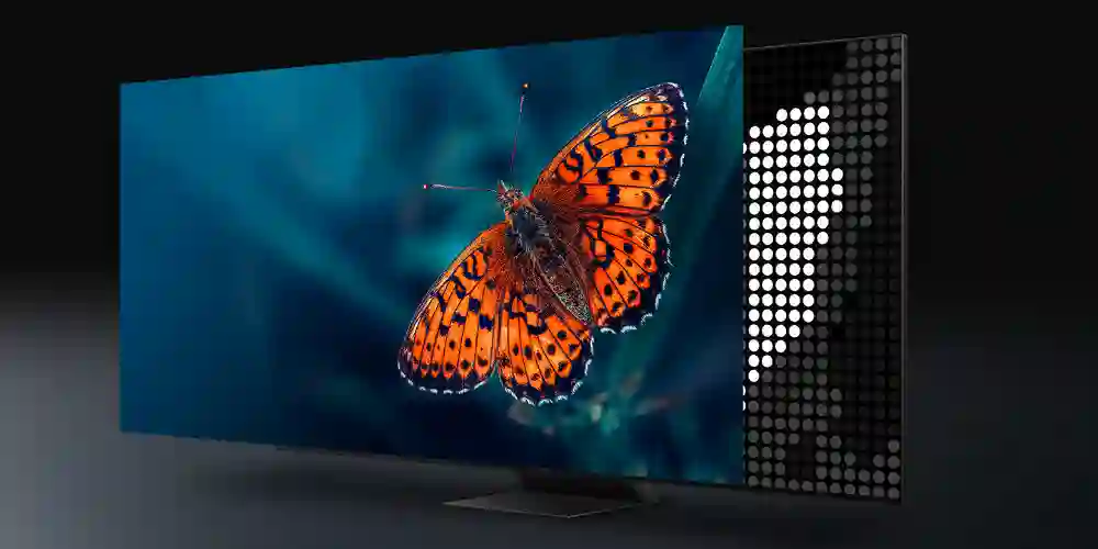
Modern chips contain billions of transistors implementing multiple processor cores, powerful graphics units, high bandwidth wireless radios, high resolution image sensors and other components. This level of integration would have been unimaginable even a couple of decades ago. A single smartphone SoC today incorporates the functions of complete rooms full of specialized equipment from the past.
Smartphones can now perform professional photography, enable high quality video calls, provide turn-by-turn navigation, play high definition videos and rich multimedia – all tasks that earlier required dedicated large scale machinery. The rise of VLSI has also transformed other industries. For instance, the automotive industry is being revolutionized by advanced driver assistance systems and self-driving technologies. Autonomous vehicles rely on automotive SoCs integrating several processors, sensors and networking interfaces to deliver advanced driver assistance features like adaptive cruise control, lane keeping and self-parking capabilities.
-
Reliability and yield
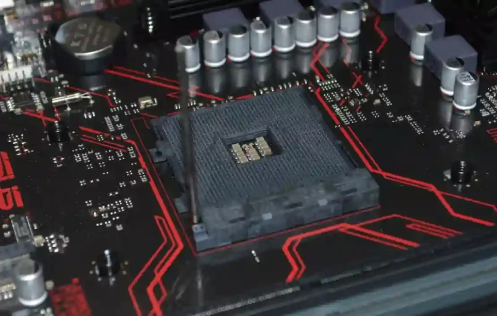
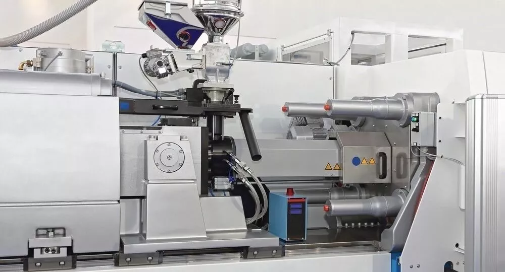
As vlsi designing allows packing more transistors into a small chip area, it becomes imperative to optimize the manufacturing process and design techniques to improve yield rates. Any defects introduced during the cleanroom fabrication can cause entire chips to be scrapped. This directly impacts the production costs.
Design for Manufacturability (DFM) principles guide VLSI designers to layout the circuits in a way that eases the manufacturing process and reduces defects. Regular placement of components ensures a uniform pattern that is easier for photolithography steps such as exposure and etching. Strict design rules are followed to define minimum spacing between interconnects and components.
This spacing becomes increasingly important at advanced technology nodes with smaller geometries as even minor contaminants can cause unwanted electrical bridges. DFM techniques also involve using larger transistors, IO pins and memory cells in non-critical areas to reduce impact of defects.
-
Performance boost
Moore’s law states that the number of transistors on chips doubles every two years. This exponential growth in integration density has tremendously boosted performance over the decades. Modern chips have billions of transistors versus just a few thousand in early microchips.
Transistors can switch at gigahertz speeds in advanced nodes. Parallel processing using multiple cores further multiplies throughput. Graphics, AI and other specialized accelerators deliver unprecedented performance. VLSI scaling continues to power leaps in computing capabilities.
-
New applications
The confluence of higher performance, lower power consumption and reduced costs has opened up new application domains for electronics. Wearables, Internet of Things (IoT), autonomous vehicles and more rely on specialized VLSI designs.
Advances like system-on-chip (SoC) and system-in-package (SiP) packaging allow integrating entire systems with diverse ICs on a single die or package. This has enabled the development of sophisticated yet affordable solutions for various industries.
-
Future trends
As transistors approach physical limits of silicon technology, new materials and 3D architectures are being explored. Multi-gate transistors are pushing further scaling. Non-silicon alternatives involving graphene and other 2D materials may take over.
Chiplet-based modular designs will combine different process technologies. Advanced packaging will integrate chiplets in 3D stacks with through-silicon vias for ultra-high densities. New computing models involving in-memory and neuromorphic architectures are on the horizon.
VLSI will keep revolutionizing electronics through the Internet of Everything, ubiquitous AI and new experiences in augmented reality. Future systems may have optical and quantum components on the same die. The role of design will become more important than ever to harness complexity.
Conclusion
VLSI design semiconductor process engineer has been instrumental in the tremendous progress of electronics over the past few decades. It has miniaturized components, boosted performance exponentially and enabled new functionalities. This has transformed countless industries and daily life. Looking ahead, VLSI will continue shaping products and driving innovation through ongoing device scaling, new materials and 3D architectures. The future remains highly promising and exciting, as design innovation overcomes physical barriers to keep Moore’s law alive.